I’m trying to build the FPGA code for RAMTester on the XEM7310 under Vivado 2019.1.
I created a project and brought in the source files and constraints. I added the MIG IP and customized based on: https://docs.opalkelly.com/display/XEM7310MT/DDR3+Memory
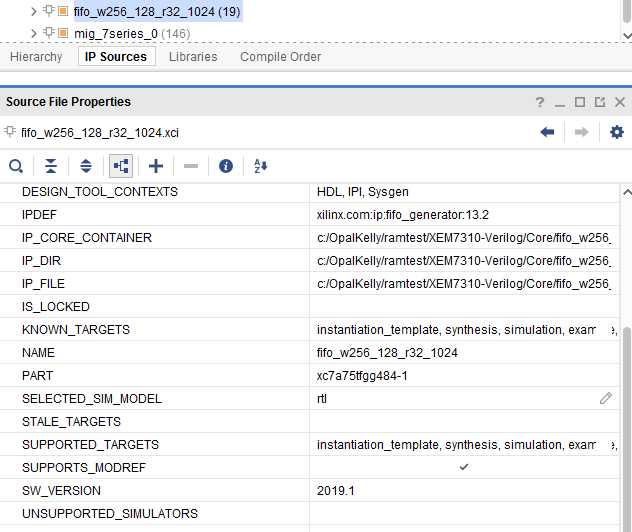
I had some initial errors as the fifo IPs were locked and out of date. I upgraded them but now when I try to build it I get:
[Vivado 12-4810] IP ‘fifo_w256_128_r32_1024’ is locked and cannot be converted:
IP definition ‘FIFO Generator (13.1)’ for IP ‘fifo_w256_128_r32_1024’ (customized with software release 2016.3) has a newer minor version in the IP Catalog. * IP definition ‘FIFO Generator (13.1)’ for IP ‘fifo_w256_128_r32_1024’ (customized with software release 2016.3) has a different revision in the IP Catalog. * Current project part ‘xc7a75tfgg484-1’ and the part ‘xc7a200tfbg484-1’ used to customize the IP ‘fifo_w256_128_r32_1024’ do not match.
I checked and they are updated. I don’t see why the project part is wrong nor where to fix that.
While this was simmering, I took care of other build errors and now it builds fine. Maybe the old error just didn’t clear. I closed and reopened the project and built it again and it builds ok.
For others trying this out, here are the things I ran across:
Copy the sources and constraints to a new location. Be sure to add the OK*.v sources.
You will probably be using a newer version of Vivado, so upgrade the fifo IP. (IP Sources tab, right click on each IP and select Upgrade)
Go to IP catalog and add in Memory Interface Generator under Memories and Storage Units.
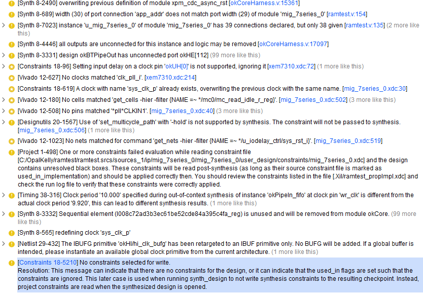
As I look at this more closely, I’m checking the many (848) warnings produced, and many look important, although the code did seem to function. Here are the synthesis errors:
Things like the number of address lines seem odd. I used the code example for the XEM7310 and generated the RAM interface based on the instructions - seems like they should match.
Generally speaking most of these warnings can be safely ignored.
In particular, the warning about the app_addr length will not negatively affect this sample, as the highest address bit will simply be ignored by the MIG core (because the MIG core address range is shorter than the other modules). Reducing the app_addr length in the other modules may reduce some utilization inside the device, but it is unlikely that it will impact anything significantly. If things were reversed and the MIG had a wider address range there would be an issue (as we would be unable to address the full memory), but that is not the case here.
Many of our endpoints generate a lot of unconnected signal warnings on okHE/okEH due to the fact that not all endpoints use every signal on those busses. These warnings are safe to ignore and difficult to remove.
Warnings from inside the okCore module can be safely ignored.
Generally speaking, FPGA design differs from software in that warnings cannot always be avoided. Oftentimes the shorthand used to make an FPGA design more readable/workable result in warnings as well (like those related to the okHE and okEH signals).
Thanks for the insights. It’s the ‘generally speaking’ that is worrisome. I suppose through testing I’ll see if any warnings are important. Your guidelines do help in ferreting out which ones I should be looking closely at, so that is very helpful, thanks!
Using Vivado 2020 with the XEM7310 board (XC7A75T-1FGG48), I built the same RAMtester project as you suggested but got stucked in the implementation part where I get this error:
[DRC BIVRU-1] Bank IO standard Vref utilization: Bank 16 contains ports that use a reference voltage. In order to use such standards in a bank that is not configured to use INTERNAL_VREF, the bank’s VREF pin must be used to supply the appropriate voltage. Example port: ddr3_dq[16] (SSTL15). However, the following VREF sites are occupied and can’t be used to supply the necessary voltage:
site IOB_X0Y161 (occupied by port ddr3_dq[17]).
Free up VREF sites or create an appropriate INTERNAL_VREF constraint.
The xdc constraint file came from the sample directory. It seems odd that if that site is a VREF the ddr3_dq[17] shouldn’t be allocated to that pad. Do you see this issue when you compile that RAMtester code?
[DRC BIVRU-1] indicates that INTERNAL_VREF is disabled. Please take note at the “Internal Vref” PARAMETER being set to “Enabled” for the MIG at the XEM7310MT’s DDR3 documentation link above. By default this selection within the MIG’s configuration GUI is disabled. Please ensure that you have enabled this setting.
I am still getting the vref error as shown below:
[DRC BIVRU-1] Bank IO standard Vref utilization: Bank 15 contains ports that use a reference voltage. In order to use such standards in a bank that is not configured to use INTERNAL_VREF, the bank’s VREF pin must be used to supply the appropriate voltage. Example port: ddr3_dq[0] (SSTL15). However, the following VREF sites are occupied and can’t be used to supply the necessary voltage:
site IOB_X0Y187 (occupied by port ddr3_ba[0]),
site IOB_X0Y161 (occupied by port ddr3_dq[10]).
Free up VREF sites or create an appropriate INTERNAL_VREF constraint.
Well the warning is informing us to enable the INTERNAL_VREF constraint. I understand you’ve enabled this in the configuration wizard and are still experiencing the issue. I’d recommend resetting the MIG’s output products and regenerating them. Starting with a new, clean, project can also be helpful to resolve issues that seem tool related.
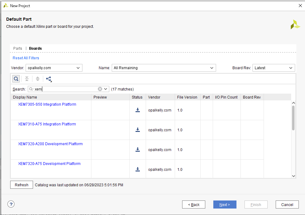
Hi, I tried to create a new post for this issue but couldn’t. So, I am posting here.
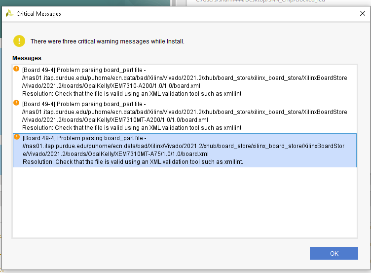
I tried to use the Board file for xem7310. I downloaded the board files for XEM7310-A200, XEM7310MT-A200, and XEM7310MT-A75. As soon as I download the files, it disappears from the option as you can see below:
I am not sure if this is a Vivado issue or an Opal Kelly issue, so I am asking in both places. The error says that the .xml file might not be correct. Can you help me with this?
We attempted to recreate your issue using Vivado version 2021.2 but didn’t encounter any problems. This might indicate the issue could be specific to your system or Vivado settings.
I suggest wiping the slate clean and starting again.:
Uninstall all our board files using the following TCL command: xhub::uninstall [xhub::get_xitems opalkelly.com:*]
Restart your computer.
Create a new Vivado project.
Fetch the latest available boards/versions from Xilinx’s Board Store GitHub repository by clicking the Refresh button.